Sonoff with external wifi antenna

not directly blynk related, but might be useful for other users, so i dare to publish here :slight_smile:

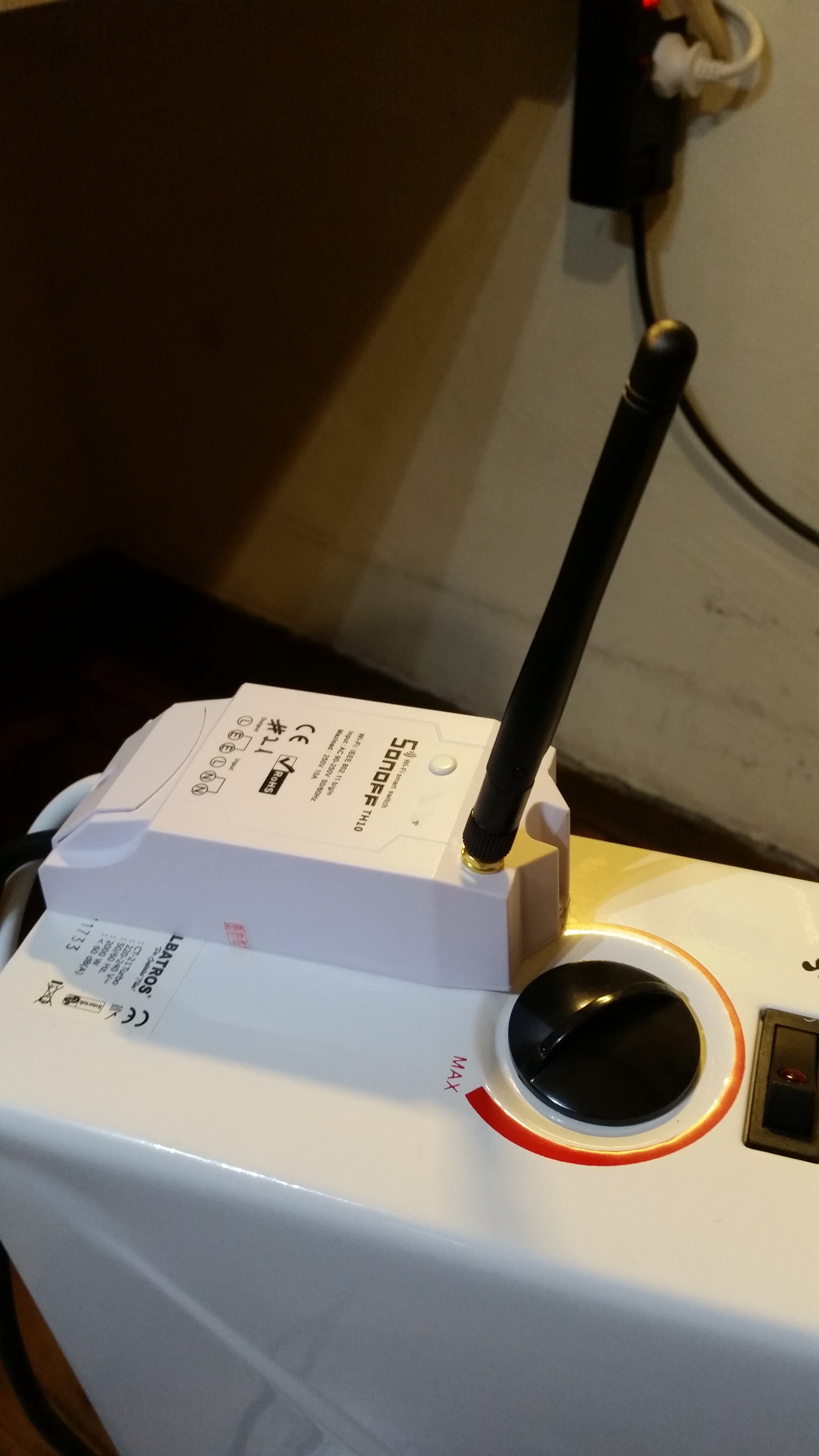
in our house, some areas have very poor wifi signal, the sonoff or smartphones could not connect at all. i had to mount a sonoff in this area (kitchen), so i thought to try to extend its wifi range by installing an external antenna. it was easier than i thought, and the end result was high above my expectations…

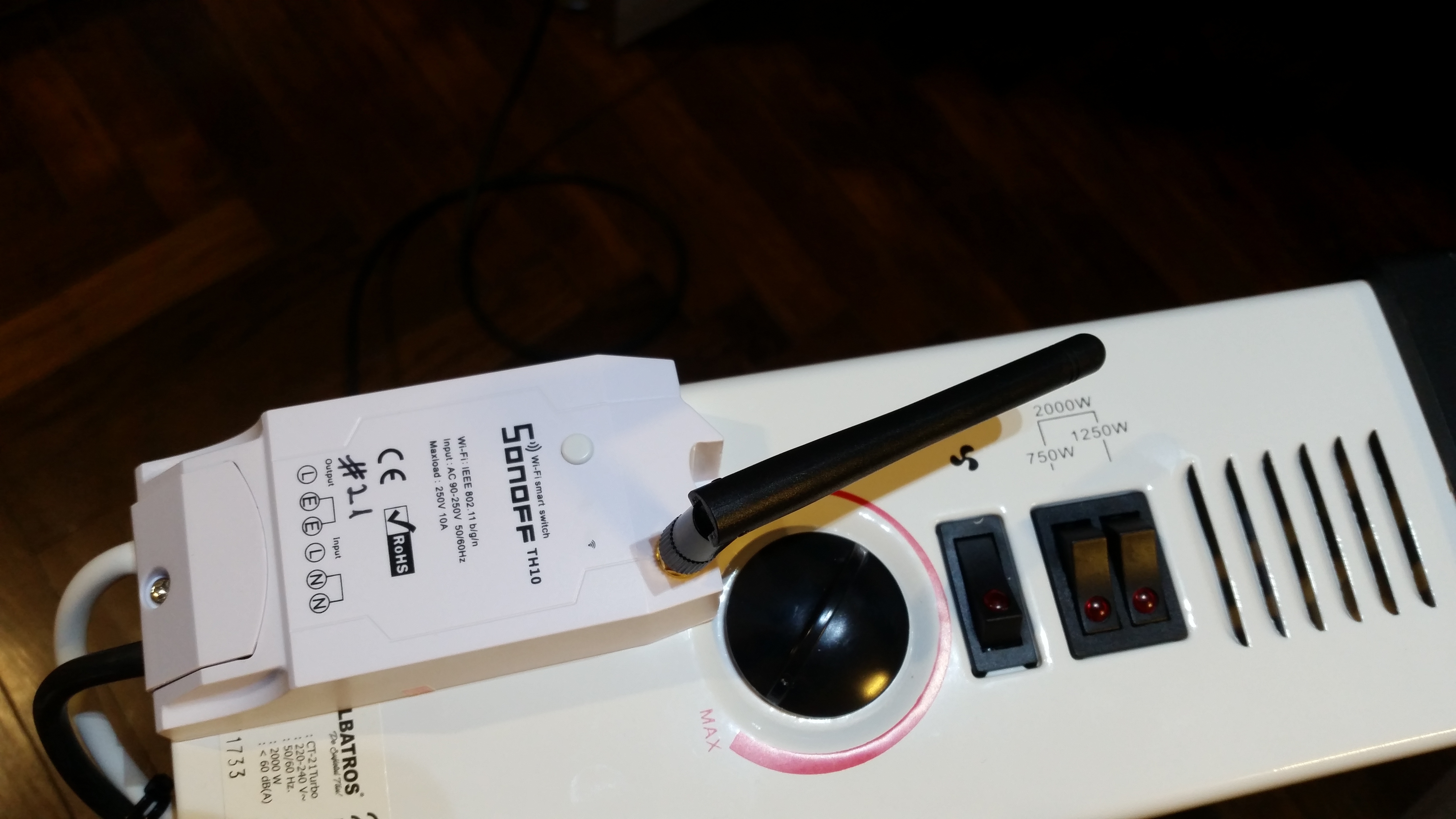
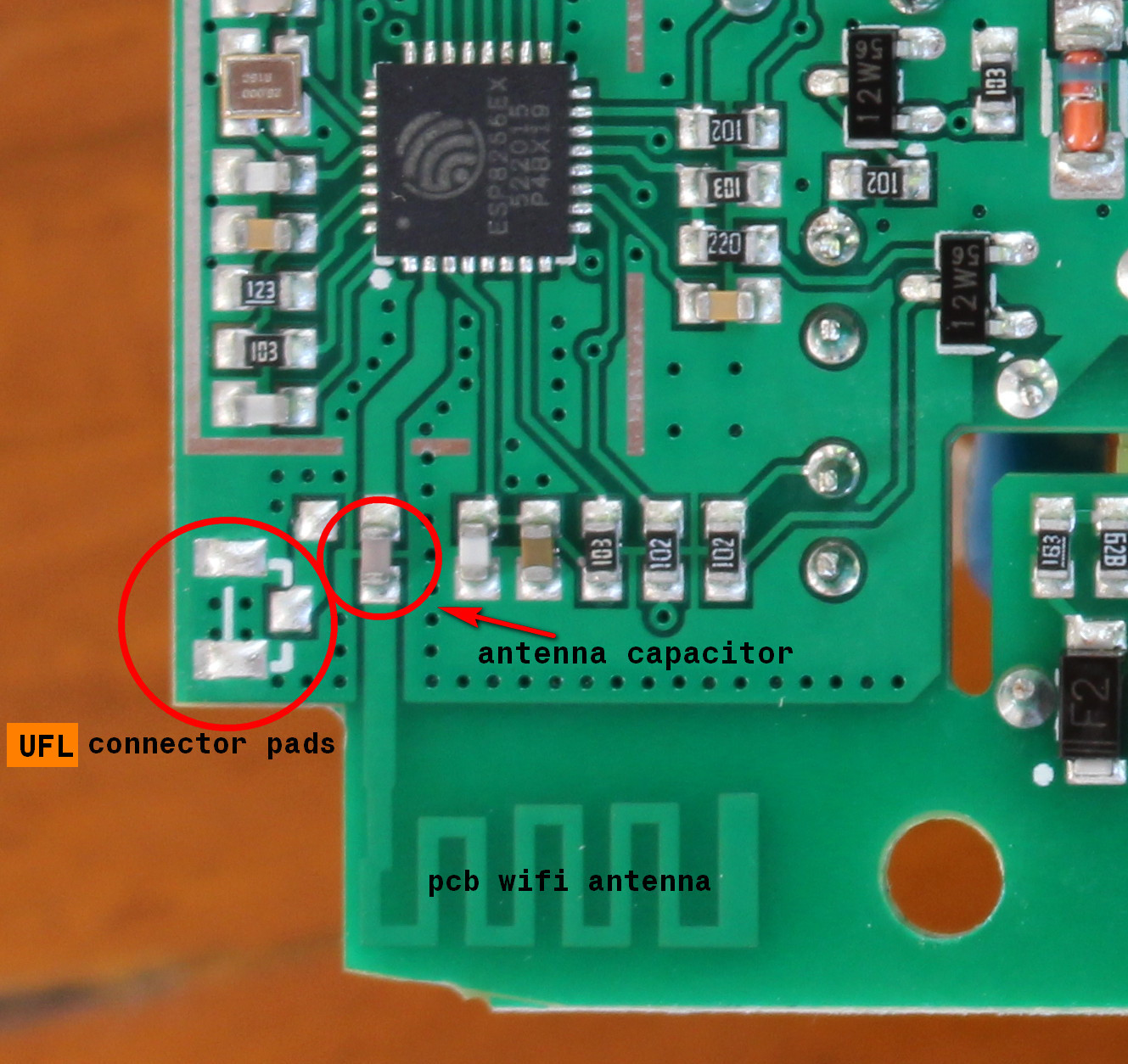
the sonoff th10 / th16 / pow pcb has already the footprint and possibility to solder external UFL antenna connector

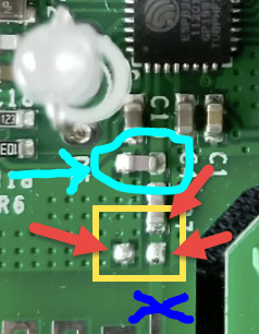
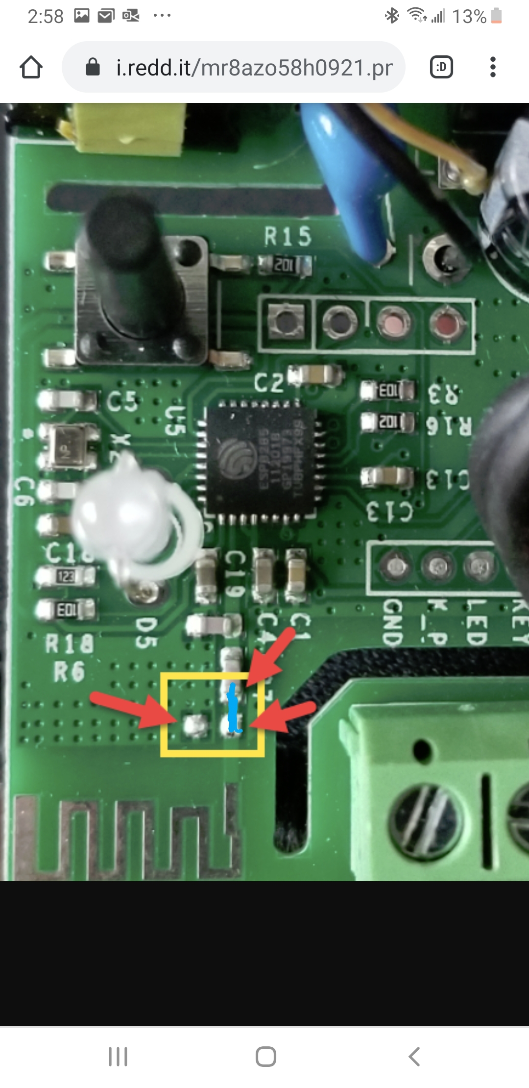
to use the sma pads, just desolder the cap, turn 90 degree clockwise and solder.

i’ve bought these antennas at ali (these are the cheapest ones, with relatively low dbm gain)

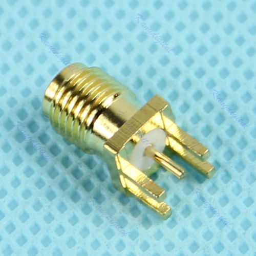
unfortunately, i didn’t had the corresponding smd UFL connector, so i just cut the coax cable on my antenna, and soldered directly to the signal and gnd pads.

after soldering, to relieve the stress on the coax cable, i fixed with hot glue to the pcb. then just drilled a hole on the plastic case, tightened the screws, and the mod was ready for testing.

i didn’t do any professional tests, just placed a standard sonoff (with pcb antenna) and the other one (with external antenna) near each other, and pushed the dbm signal values to the phone every second.

the external antenna showed in average a 8 dbm stronger signal! -90 vs -82 dbm. considering that every 3 dbm doubles the signal power, i think this is a very good result.

the unit with the external antenna, managed to maintain a stable connection, versus the unit with pcb antenna dropped the connection quite often. and, as i mentioned, this is a relatively low gain antenna, there are much strongers on ali for some euros more.

8 Likes

Can you show us the finished product inside with the SMA connector? I think it would add to it.
smapcb

i would, but as i wrote:

i didn’t made a photo about the soldered antenna cable to the pcb, and the unit is already mounted on his final location, which is not accessible for me.

but it is not hard to imagine :slight_smile: just solder gnd to gnd and antenna core to the middle (smallest) pad.

the proper way would be to solder to the pcb something like this or this, but i didn’t had at hand at the moment. (it is the same connector used in laptops or mobile phones for wifi / gsm)

http://uk.farnell.com/productimages/standard/en_GB/1688077-40.jpg

1 Like

Yes, that’s the proper type of connector to solder onto that pad arrangement.
Because the pads are near the edge of the board it looks do-able. I once tried to solder one of these onto a board where I had limited access and managed to get a blob of solder down the middle of the socket. By the time I’d managed to de-solder it I’d applied too much heat and the tracks were lifting off the board!

Pete.

yes, for soldering smd, it is ok with iron, but for desoldering smd components with more than 2 legs in non destructive way, it is better to use hot air.

1 Like

Okay, the pcb label is incorrect then. It’s ufl instead of sma. UFL is much smaller. Anyway sounds like you’ve got it. I’ve used the sma ones on some other projects. The UFL ones are used on variations of the ESP modules.

1 Like

i see. the label on the photo was made by me, i’ve thought it is called sma, because the seller on ali advertised like that. but i will correct the photo than.

this was the source of confusion. thanks for clearing this up!

2 Likes

All these posts about Sonoff is making me want to play with one. They’re inexpensive enough.

Great job by the way!

1 Like

Great photos!

Just ordered a bunch of UFL/IPX flexible antennas and connectors from Ali ($3 total).

I have a sonoff pow “rev2 v 2.0”, which has no more the UFL pads!
Suggestions about how to solder here an UFL connector?
I think soldering coax cable directly to PCB would cause great attenuation of signal!

https://jumpjack.files.wordpress.com/2019/01/fri-jan-04-163108-gmt0100-2019.jpg

Are these the pins for an ipex/ufl connector on my sonoffs?

Subscribing.

hey!

probably you can easly follow the traces on the pcb, there should be a small capacitor between the antenna and the mcu. if you take a look at a esp8266 pin map, you can identify the antenna pin.

you can find the official schematics for all sonoff proflducts on the itead website.

According to this schematic, the capacitor marked C27 (10 pF/50V) is the one connected between the ESP8266 and the PCB antenna, so it looks like you’re on the right track :slight_smile:

But the encircled (turquoise) SMD doesn’t add up with above schematic:

image

If I had to guess I’d say it’s an inductor that helps tuning the antenna (a.k.a. “antenna matching”) to the receiver (because it’s connected to GND) , but I’m not sure. Normally there would be two inductors and one capacitor (or vice versa). Or a resistor… Building antennas and antenna matching circuitry is a black art. If it was the dark ages you would probably be accused of witchcraft and burned alive if you had something to do with it! :smiley:

Aaaaaanyhow… In these low-end circuits with limited wattage, the performance is what it is. But as opposed to @wanek 's PCB, you can’t just flip the capacitor and add the connector. From what I can see on the picture, you have to physically cut (at the blue X) the path to disconnect the PCB antenna. Then you can solder a short coax cable to the pads and then to a connector. Looks like bottom left is GND.

Good luck!

When you say “then you can solder a short coax cable to the pads…” , are you referring to the 2 pads running in line to the PCB antenna?
Connect the 2 pads with a short coax?
A bridge?..marked in blue.

Youll have to bare eith me, im new to PCB jargon and im sure I didnt use the right terminology.

Coul you not just use solder to bridge both pads because they are so close together?

Thanks.
G.

I think you’ll find that the two pads that you’ve drawn the blue line between are already connected - easy to check with a continuity meter.
These are the active side of the antenna connector, and the other pad with the arrow pointing to it )the one on the left) is the ground side of the antenna.

In practice, simply soldering a wire to the active side is what you could do. The other end of the wire would be unconnected. I’d prefer to solder a male UFL connector between the ground pad and the active connector, but because Sonoff haven’t provided a property UFL pad layout you’d need to take care to get the connector oriented correctly and you’d probably need to scrape some of the green solder resist off of the ground plane area to provide a good mechanical fixing. Soldering the UFL connectors needs a steady hand and a fine tip to the iron (and a good magnifier in my case), as it’s very easy to ruin the connector by getting a blob of solder inside the socket part of the connector.

Either way, you would need to cut the track that leads to the PCB antenna, in the place where @distans marked with a dark blue “x” in his photo.

Pete.

I really, really do hate antenna circuitry! :smiley:

Looking back at this, I might have to change my answer to “decoupling capacitor”. But it’s still a black art! :wink: