Hello Guys,
I have made an board by using this board we can control up to 4 Appliances via Relays & also we can monitor room temperature & Humidity via DHT 11.
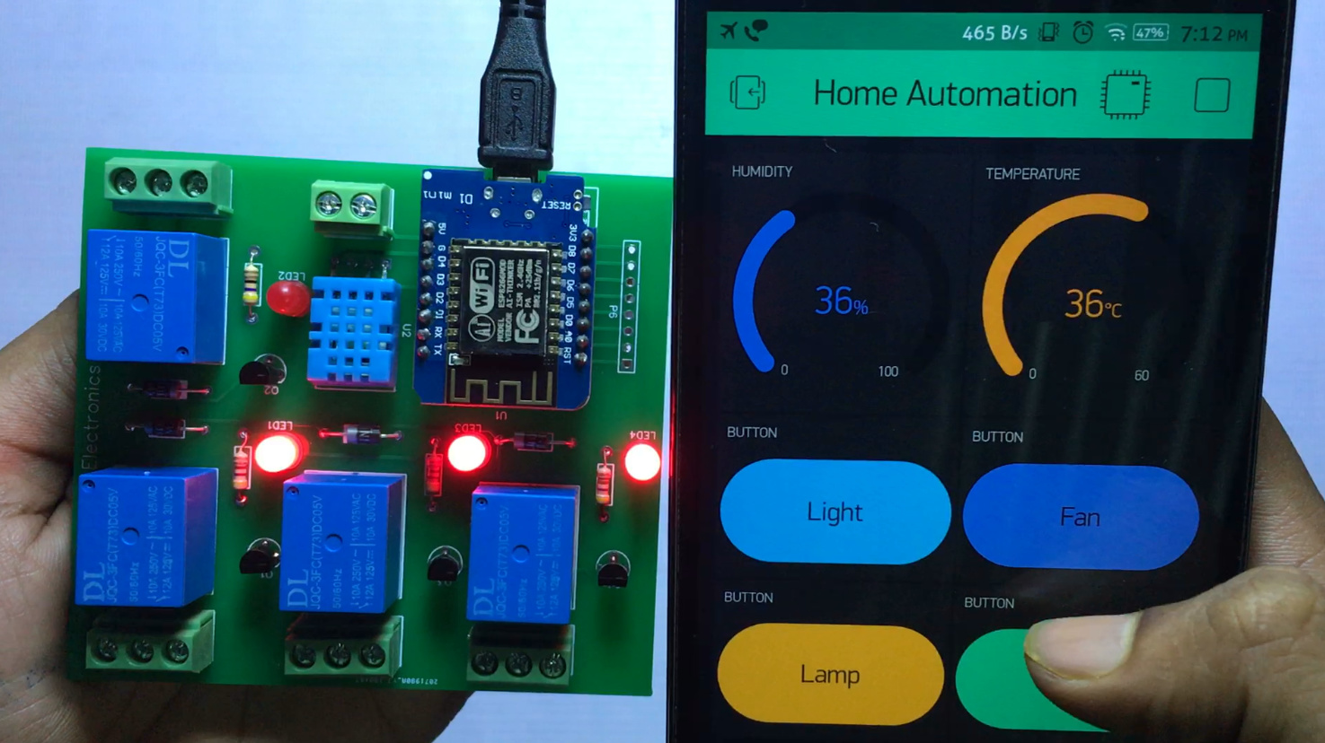
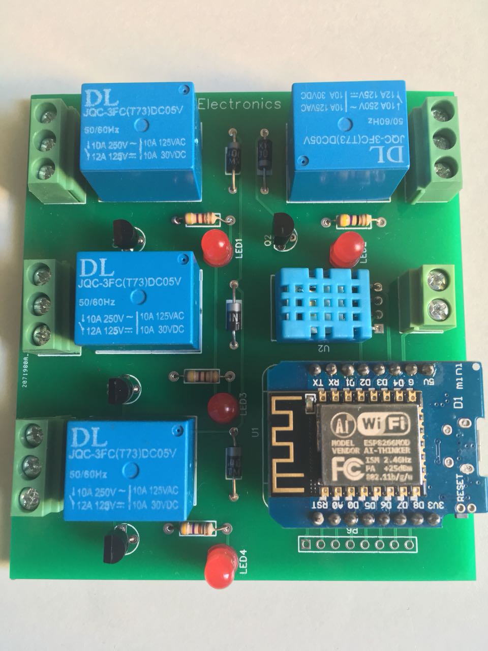
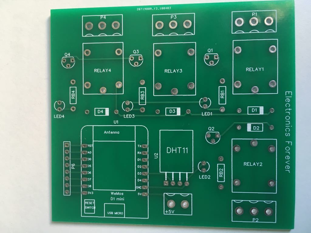

Previously, I had made same board by a manual etching process
Hello Guys,
I have made an board by using this board we can control up to 4 Appliances via Relays & also we can monitor room temperature & Humidity via DHT 11.
Previously, I had made same board by a manual etching process
Very cool! Thanks for sharing
nice video, good work!
next time use “copper pour” for gnd plane, it is good for the circuit and also for the environment - it produces less toxic waste, and the boards look more professional 
also, try diptrace pcb design software, it is very user friendly and completely free!
@saurabh47 Nice!!.. I like how you showed, step by step, the App project setup. Much more beneficial for learning then posting a simple QR 
Thank you so much to everyone.
Can you explain in detail How to use “copper pour” for gnd plane,?
I will take care of it.
Copper pour is when the unused copper plating is left on the board. Your PCB layout program may have an option to do that.
i would, but i’m not familiar with the design software you use. you should google it.
I’ve always thought that using copper pour in the area where you have an ESP dev board mounted will reduce the effectiveness of the onboard antenna.
Pete.
Also, it’s not clear how large the tracks are that handle the mains power, or how much physical separation there is between them and the low voltage connections to the relay. If you take a look at some similar boards such as the Sonoffyou’ll see that additional so,Der is flowed over the mains tracks (which are already quite wide) to beef them up, and parts of the circuit board are routed out to provide an air gap between the HT and LT sides. hT tracking across the surface of the circuit board can be an issue in high humidity or dusty environments.
Pete.
The tracks is 1mm large, so no enouth power, for 2oz of thickness only 4A.
true. but in all programs it is possible to delimit the copper pour area. or, it is even better if the esp board is mounted so in the pcb to poke out the antenna part.
regarding the required trace clearence and width for high voltage / current, there are concrete tables and calculators on the net, so this can be designed properly.
there is a quite good free pcb design tutorial, by dave jones (that crazy austral guy). it is a bit outdated on some aspects, but it is a great starting point. i’m on phone now, i will try to find the link.
here it is:
http://alternatezone.com/electronics/pcbdesign.htm